
System Cost, Module Prices, and Quality Considerations of High Power Modules
Benefits, Risks, and Costs of Large Format PV Modules
Almost all leading solar module suppliers have now unveiled PV modules above 500 W. These high-power modules use a combination of technology upgrades at the ingot, wafer, cell, and module level, striving to achieve higher powers, and in some cases higher efficiencies.
Specifically, manufacturers are achieving these wattage gains through half-cut or even triple-cut cells, multi busbar ribbons, dense cell-to-cell interconnection, larger wafers, novel module layouts, high-efficiency n-type cells, and other innovations.
This new generation of high-power modules can lower price/watt of solar in several ways, but that assumes that these new products and technologies remain consistently reliable, and the entire solar supply chain can efficiently, and cost-effectively, adjust to compensate for larger and more powerful formats.
Furthermore, high power modules also pose additional risks to certain cost and mechanical areas and are likely to carry a small price premium during initial product launches given the potential for such modules to provide additional balance of system savings.
In this webinar, we cover what to expect in the coming year as high-power modules continue to roll out. What are the capacity forecasts, cost and price drivers influencing supplier decisions, the technological benefits and risks, and what precautions or adjustments asset developers and owners should consider when purchasing high power modules.
Moderator:
Michael Schmela, Executive Advisor and Head of Market Intelligence, SolarPower Europe
Speakers:
George Touloupas, Senior Director, Technology and Quality
Joseph Johnson, Senior Technology and Quality Analyst
Podcast Transcript
Michael Schmela:
I'm very happy to welcome you to today's Solar Power Europe webinar with our members. For many, many years, module technology was somewhat boring. Not too much has changed but that has changed quite a bit in particular over the last two years as much to play. As a means to increase power ratings too. Yeah. Pretty high-level or they haven't come to an end, probably. So, we are very happy to have today CEA present to us on high power modules, system costs, module price, and quality considerations. So basically, all you need to know on this last, and we have two presenters from CEA, the first presenter will be George Touloupas, who is old friend of mine and the senior director of technology and quality solar and storage at CEA. And we have with us also Joseph Johnson who is a senior technology and quality analyst at CEA, so we'll start first with George. George, the floor is yours.
George Touloupas:
All right. Thank you. Thanks to everyone for joining this webinar on some really hot topics. So, without further ado, we have a lot of content to share with you, and very good to also hear your questions. We're going into it. So, talking about higher power modules and replications of system, cost quality for the module price.
Clean Energy Associates (CEA) Company Snapshot

A very quick pitch on what CEA is and does. We're a technical advisory and a quality assurance company where we have a global footprint with engagements, more than sixty countries. We have 13 countries with a physical presence, a very long 13-year track record with close to 150 professionals. Most of them are engineers and a millennium plus years of industry experience with lots of experts. So, we do that for solar and storage supply chain management, engineering services, quality assurance, and market intelligence. That's all you need. So, it's a rectangle of services which is very important to take the right procurement decisions. And we have a very strong track record with more than 85 gigabytes of projects in total, and more than four gigawatt hours of battery storage engagements, and all of these in hundreds of factories for batteries and PV inverters modules and manufacturers worldwide. So, I will present the technology part and then we'll do the pricing and updates.
High Power Modules - CAPEX Advantage

So, let's start with a very brief overview of the changes that have been happening in the last couple of years, ramping up a lot in the last year and after a very long sleepy period like Michael said before, everything changed and still changing very fast at a very fast pace. So, this has not happened before. If you look on the right-hand side, we want to reduce CAPEX in this industry. I would want to do that, of course, to reduce the LCOE. CAPEX is the module and the balance of system, roughly this proportion, give and take. Now using technology mainly three free toolboxes, the wafers, the connection, and high efficiency. You can reduce both the module cost and also very importantly, the balance of system costs. So larger wafers impact the module cost, the bowel system costs because you have more wattage upon them. Density under connection increases the efficiency or the area of issue of the modules. So, getting more module efficiency ratio increases that, but also besides decreasing the module price, it also decreases the balance of system costs. And of course, with higher efficiency cells, you can have all the above benefits combined. All this is of course, to reduce the issue. And this is the same information, but from a supply chain, a view perspective. So, on the policy side, there is nothing new really except the very intense price hike, but it's not related to technology, but going on the angled and downstream, a lot of chains.
High Power Modules - Changes Across the PV Value Chain
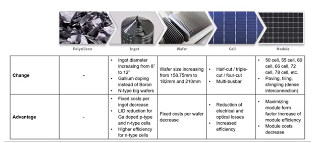
So, ingots are getting very big, really big. And the limit is 12 inches, which is what the semiconductor industry has been using for many years. So, the previous sectors decided to use the biggest available size. The other big change is that gallium doping is becoming the mainstream way of doping across the industry very, very fast. And of course, in time, ingot sales will gain because the fixed cost bring LID reduction, higher efficiency, of course. And on the wafer side, bigger income means bigger wafer. And fixed cost per wafer decrease.
High Power Modules - Ramping up Capacity

On the cell side, we have a lot of innovation. A lot of things happening in half cut, triple, four cuts, which is a new variant. We just saw at the SMEC show in Shanghai were, a big team there, unfortunately I could not because of COVID restrictions. These all have a great benefit, reducing electrical, optical losses, increasing the overall efficiency on the module. Even more variation in innovation, huge range from, for the number of sales from 50 to 78. These are full cells. So, if you got them, you double if you triple cut them, you triple them. And of course, paving, tiling, and shingling are very prominent. So densely packing the cells in, more intense fashion, increasing the module efficiency and decreasing the marginal cost. And there are two camps. They formed last year around about a year ago, we entered the G 12, and I'm fairly sure it's 182 millimeters. And G 12 is short for 210 millimeters. Basically the 10 and 12 are the diameter of the ingot in inches. The G 10 was decided like a year ago. The G12 was decided several months before. So even the wafer sizes were not fixed a year, year, and a half ago. And now they're talked about as a standard. That's why we have these accounts, these alliances, because it's very important in this industry to standardize everything and streamline the supply chain. That's how you bring down the cost. So, on the G12, we'll have Trina and Risen, the main proponents, and the M10 or 182 JA and Jinko can launch.
Of course, there are others that are following and joining sometimes both of the alliances. But I would say these are like the first cameras, the biggest players, and other capacities also significant, and the roadmap still points to 210 millimeters. We don't see a bigger way for coming in soon. So, what we will be getting is a higher power from higher efficiency and not from higher format, a bigger format or bigger wafer size. That's what we expect to see. And N6 which launched like couple of years ago, it immediately became a transition wafer size. So, we expected to speak to stick around for a couple of years. It is until everybody migrates to either M10 or G12.
Constantly Evolving Wafer Size Alliances

Now we talked about the alliances before, we're going to give some more depth and insight here. The interesting fact is that the leader of the G12 Alliance is Zhonghuan who is a pure-play mono wafer supplier originally strictly in the semiconductor industry. And they entered the PV sector a few years ago through their partnership in China. And they introduced the big 12-inch ingot diameter and the big wafer size to the PV industry, but they already had these for the semiconductor industry. So very big capacities, 52 gigawatts adding another 23 until 2022. But LONGI is definitely the leader with 89 gigawatts of capacity.
So, we can discern a trend here. The suppliers with the big ingot or upstream capacity, they are the ones that have opted for a M10 wafer and the averse, the proponents of the G12 they don't have upstream capacity. They don't have ingot capacity so they're basically buying from Zhonghuan. Okay. So, it's a very different, the two accounts are very different with that respect.
Dense Interconnection Technology Updates
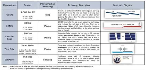
A few words on the density connection technologies I would say it's tiling, paving, shingling right now. Tiling is promoted by Hanwha, JINKO originally promoted it, but they had pulled out of tiling to a great extent as they didn't see that as beneficiary compared to the production issues that it caused. We've learned very recently at the SNC show that the JAA is also promoting tiling. That's a recent event captured here. So, with tiling, there is an overlap on the cells. In a sense it's similar to shingling only you use soldiering instead of electrically conductive based. So, it's good old, well-known conventional, soldering. So, this way you can have very high area efficiency. Actually, it's the highest by using tiling or shingling. It's hard on paving, but by a tiny amount, but the most popular by far is paving where you still keep some distance between the cells. And just to remind everyone or let everybody know that the conventional module has a two-millimeter distance between themselves. And there's a good reason for that because when the ribbon flicks from the front to the back that could be some stress on the edge of a cell that can create cracks and other issues, we'll see that later.
So, if this reduced to half a millimeter, close to half a millimeter, of course you can pack more cells on the same module area, increase efficiency and bring down the cost. And all these benefits that we discussed before. For a lot, you probably need to do something in the area between the cells. So, I either used a segmented ribbon with different profiles, different sections or formula ribbon during production and flatten it like what Trina is doing, for example, pinch it. So, it's much thinner and it does not stretch. So, and shingling is the other a very well known, very mature interconnection technology. It's mainly its main proponents SunPower has the IP, the Chinese module makers do have some shingle capacity and there were presenting shingling modules for many years now, but they kind of pulled out from that and focused on the more conventional soldiering method of putting cells together, but with reducing the distance. So, achieving more or less the same effect if we use half cut and multi-master same efficiency.
Paving Technology - Risk Analysis

Some risks when you do all these things, as we said before, with paving, the distance is reduced, and you have to do something there. So, we kind of covered that before. So, either use segmented ribbon or flattened ribbon to avoid stressing. Now in the middle, you can see what happens when a cells cap has been cut for many years now in mass production. And right now, there's practically no full cell, everything's half cut. There were many problems as we were following this with manufacturers and the R&D product teams, initially a lot of manufacturers had big issues and they avoided cutting cells. Now more or less that has been solved, but still the conventional laser cutting with technology creates a picture like what you see in the left. So, it's called laser ablation. So, the laser destroys a big part of the silicone.
This is around 180 microns. So, one fifth of a millimeter it is very thin, very fragile, and that would reduce the mechanical strength. So, the new damage-free cutting technology does not do that. It gives a very nice clean area. So, it has a big advantage. It increases the strength. So, we need to have strong wafers that are not susceptible to breaking. Especially one that has a very small distance between the cells and there is a piece of metal there that stresses them, even if it's a little. Also, the role of encapsulant is very important no less than for protecting the very fragile and tiny rebond that are being used instead of flat, Y busbars that where the mainstream like one or two years ago.
Reliability - Junction Box & Diodes

So, the encryption and thickness are critical as well. Also, the quantity of the encroachment. There was another discussion regarding the junction box and the dials mainly because of the Z 12 modules that have by design higher current it's around 80 NAMS. And you have to add the beneficial boost to that if the module is bifacial. So, for these modules, a new generation of junction boxes had to be created. There were fewer products, fewer suppliers now it's getting better. And the proponents of the G12 camp, like Trina Solar advertising this to a kind of decrease concern out. Now the truth is that even if one uses the 30-amp, diode there, the safety margin is a bit smaller than the M10 modules that have lower current. So, this is a concern, but with the right testing. And of course, the right production methods, this would be alleviated. The process, even if you do all the testing and everything goes fine, the processes very important. And if you have seen PVLs 2021 scorecard. They mentioned clearly that junction box keeps failing and more and more. So, there is a problem with junction boxes, and they're not made as good as they should, or even not only for the design, but also the process. So, this is something that needs attention and it's a fairly easy fix.
M10 vs G12 Comparison

This is a kind of heatmap off M10 and G12 products that have different variants. Again, the number of cells is not reflecting the full cells. So, these aren't really half cuts. All of the M10 modules have a lower bar class and the G12 has higher by the results of 55 Cell variant, which has the same weight, like as the M10 products. Now, these changes in design have more impact on the G12 products. We discussed some reasons why this is so. Before, for example, the first row talks about the junction box and diode, and this is a medium level of risk. But, you know, we have to be mindful of that on the balance of system. We have changes for the fuses, of course, higher current means possibly bigger cable or our losses threading compatibility, mainly due to the length which can be impacted.
It could be unsuitable for high wind or snow regions because, it can be overwhelmed or a zeroed by putting more still on the track, your own structure beneath and also mechanical loading tests are very important. The module has to be tested on if you use trackers on rail of the tracker or not. On a generic structure, it can have very different behavior. Shipping more or less has been resolved. So, it is spiking G12 modules vertically. So, there's a lot of innovation to solve these problems and it's getting better. So, this was more read the last quarter, it gets better. I'm talking about the right-hand side of digital modules. For the trackers as we discussed before, there is a lot of evolutions or more tracker designs that accommodate bigger modules are out in the market now.
Large Module Tracker Solution
But there are several modifications that need to be done. So, the railing must be increased. The height of the piles must be increased. The gaskets must be reinforced. And as we said before, depending on the load that is defined really by the conditions of the project relegation, there might be a need to increase the amount of fill use, and that can have repercussions on the bottom. So, system savings that were originally planned. And as we said before, for the mechanical load, they might be tested on the actual preparation and not the standard fixed mount configuration. And this manufacturing must use the right frame designed thickness and allow to make these modules suitable and bear the loads without bending or breaking.
Risk Mitigation: New PV Module Technologies - Mitigation Plan

So, to mitigate all these risks, a buyer should take some steps that are easy to do. They look complicated, but really, it's a series of steps that if they're done in the proper way at the right timing, all these risks can be mitigated to a great extent. So, at CEA, we have a process that we call the golden standard, the presets of the product qualification requirements and production requirements, and the quality assurance, right at the beginning, even before the contract is signed. It's kind of upended, it's a technical appendix to the contract, it takes care of external testing, and which is a higher risk area. That's why it has a red dot next to it. With very brand-new designs, including their bill of material combinations have not been fully tested. So, lots of gaps. Nobody's happy about the situation. We understand that the manufacturers have to spend way more money testing and these tests are very lengthy.
They take six or seven months, but on the other hand they are a must, they have to be done because I see certification testing is not enough. This has to be reviewed so the bill of material review service was really looking at all the testing reports and making sure that the bill of material matches what has been ordered. And the results are good. We don't see any failures there. And as soon as this has been vetted, of course, the factory must be audited and production processes, especially if it's a brand-new line or a brand-new process. And so, on when the project is actually manufactured, the module manufacturer, you have to be there and make sure that all the material subjects are checked. For example, that encapsulate is 600 and not 500, because that makes the difference. And it's of course the right product type, down to the inspection and batch testing, where you pick a couple of modules, everything is testing or hail testing, if it's in a severe failure.
M10 & G12 Alliances Compete in Claiming the Highest BOS Savings

So, we'll go ahead. Right. A few slides here looking at these claims of high savings and the fight between the N10 and G12 alliances because it's all done to reduce the balance of system cost. The baseline is the M6 wafer, and the comparison is done between M10 and G12 and M6.
Modeling the BOS Cost Savings: Project Conditions

So, this is a qualitative analysis. It doesn't have figures because this is very hard to do. It's not an illustrated calculation but I think still there are some useful conclusions. The modern project in Spain is 110-megawatt DC. The temperature range is from 0 to 40 degrees, and there are four cases for one portrait tracker short and long one, and a two P tracker had an, a fixed configuration.
Modeling the BOS Cost Savings: Project Conditions
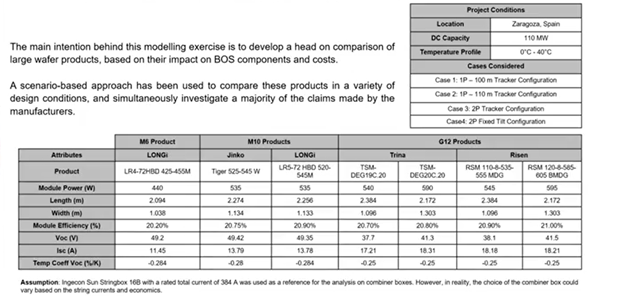
So, let's see how they perform. These are the modules. We're looking at an M6 product from LONGI as a baseline and two M10 products from JINKO and, or G12 variant from Trina. Module efficiencies are more or less similar, except of course the M6 and now looking at the power classes, they're very different, of course. But as we said, the 70 cells, the M10, and the 55 cells at Trina they're very similar. Also, they have the same width, very close. The factors that affect the savings are marked here in red, also VOC and ISC. You see the current digital products being very high.
M10 Products appear to have an Advantage with Existing 1P Trackers
So, it seems that for existing 1B trackers, the M10 products have an advantage. You can see that from a heatmap. So, the greener, it is the more advantageous it is. So M10 products have more power for this tracker. Existing means that's a hundred meters, so it's not an extra-long. It's not a new generation of trackers. Let's track your units. Overall better length is less, savings on the pile’s slight penalty on the combiner boxes. And then upon the foundation is still most morals, the same the DC cabling, they're in the same range, both solutions. I mean, and as we discussed before for the general safety, now we have lower safety margins. Again, this is not a deep red, it's just a concern that can be solved with the right testing, et cetera.
The Longer 1P Tracker Axis Largely Favors the 55 Cell G12 Products
You can also observe others, a higher tracker length utilization for M10 products, and that's part of the benefits come from. Now, the longer 1P tracker axis favors the 55 cell G12 product will have 45% more power per tracker, which is a lot. But there is a big penalty on the combiner boxes. So really this is not about numbers and cents per watt. It's more important to statement, but you know, there are some savings here that can be done. And the areas that are more few are shown in green or deep green. The string length is reduced to accommodate three strings per tracker. So, this has been tweaked to optimize the solution.
Mainstream p-type and n-type Solar Cells
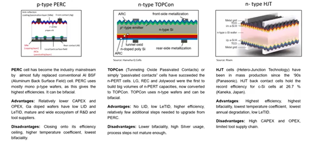
And now for a 2P fixed tilt, this largely depends on the project site conditions. There is no clear winner here. So, it's keeping to the end type section. Of course, you're welcome to send questions here and we'll be very happy to answer. Going to the N-type section this is the picture on the left-hand side, we have the workhorse p-type PERC has relatively low CAPEX and OPEX on these lines. And then we'll have gallium dope wafers, either big improvement, but it's reaching the efficiency ceiling. So that's why everybody's looking at N-type now. Top contender for hetero junction. They have a better passivation on a perc. They have to use N-type and bulk wafer because that's the best application and gives a higher efficiency.
The Race Towards 24% + Efficiency

Some of these will have additional steps compared to PERC, they use a lot of silver. The process steps are not mature enough. The bifaciality is not as high as desired for cost issues. And on the right-hand side is like the crown of silicone. It's the heterojunction, the highest efficiency cell. It's about compacted junction that's champion. Of course, but it has a lot of issues with a high CAPEX and OPEX limited to supply chain, all of these lead to a higher cost, but we expect these problems to be solved by pioneers that are really focused on that. So, the whole idea is to go above 24% because PERC cannot go above 24%, that's the theoretical limit, as you can see on the table on the right. Yeah. It's 24.5 actually, but that's theoretical.
That means when you do production, you are going to have a lot lower number because it's not economical as you go there. The difficulty towards the ceiling increases asymptotically. TOPCon has surprisingly higher vertical efficiency hetero junction, but as we said before, that's theoretical. But that's cool. That's actually surprising to see that it can go as high, but both of these technologies can lead us to a much higher efficiency than the current ones. And then past that we'll have perovskites in tandem. Really quick, now our conclusion is that it's a lot easier to upgrade an existing PERC line to Topcon and a brand new TOPCon line has a similar CAPEX, a bit higher, but it's a lot easier. It's a lot more difficult to upgrade per client to hetero junction because you really have to drop the most expensive equipment.
n-type Technologies: Progress and Adoption
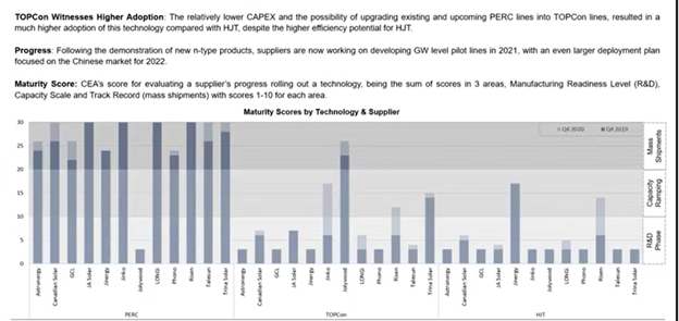
And hetero junction equipment, the CAPEX is here higher. So brown fields, existing pipelines will probably go to TOPCon, but brand-new investments might also be hetero junction because of the efficiency plan. That's what we see being planned. That's another interesting view where we see the progress in adoption. This is a maturity score based on the methodology that we have developed last year in our supply market intelligence program, where we have zero to 33 score areas from 1 to 10. So, if you add all three scores thirty, which is when you have reached mass shipments. So, you see the changes from 2019 to 2020, big changes or small change for PERC, but relatively big changes for JINKO, Longi, and Risen, going towards TOPCon and for hetero junction, well, it will change actually it's actually more reason getting more progress here. I guess now, if we did that now, after VSNVC, we would raise considerably Longi's TOPCon score as they launched a TOPCon module. So, there's a lot happening now on this front, and of course we bump even higher. So that kind of depicts the movement.
Cell Efficiency Comparison - PERC, TOPCon & HJT

This is another interesting chart tracking efficiency, mass production efficiencies for PERC. You can see them reaching 23% for Topcon, but really not. The light blue is a champion or R&D, but Jolywood has achieved 24.5%, which is impressive. So, closing to a 24%, this is very important, but on the hetero junction relates only energy and reason about the capacities are very, very small. And there are difficulties we'll discuss before CAPEX.
Supplier Cell Capacities - TOPCon & HJT

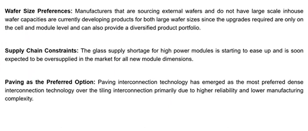
TOPCon is really top with NLG the most mature by far, there are some pretty solid managements by origin, for example, but we have to see whether this materialize, and hetero junction REC has the biggest announced and that's for 2022 actually because we'll get plants, I think seven gigabytes in a few years. So, a lot of movement, but still, this is far, far below what PERC is doing, but as expected, when something's successful, it gets rolled out very fast. Now key takeaways, supply chain bottlenecks could impact higher power module production because bigger sizes require bigger, wider back sheets, bigger glasses, wider glass, et cetera, or new type of junction boxes. These supply chains shortages constraints are being eased out now, especially for the glass, and also see that paving is a preferred option because, because it's easier to do and it gives a pretty good benefit.
Key Takeaways: Supply Chain Bottlenecks could Impact Higher Power Module Production in 2021
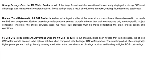
Now looking back this analysis, we did the choice of the whole month, right? So, on the project specifics, it's not an easy decision. There's not a clear winner. Of course, they are both better than M6, this is clear. The 55 and G12 looks like it has an advantage over the six seven, which is wider and has some impact on some panel balancing savings. Regarding the end type, as we said, Topcon looks to be a to winner because it's a fairly easy, not so easy, but it's easier on hetero junction going from PERC to Topcon.
Key Takeaways: The Choice of the Ideal Large Format Module Relies upon the Project Specifics
And the outlook is that hetero junction is much lower key, only Risen and Jinergy have announced the capacity development for 2021. And this is because of the CAPEX. And PERC is alive and kicking extended runway with them. Two, three years, we don't really know if TOPCon's successful. If everybody, we will transition there very fast, like they did from only conventional PERC cells in two, three years. And with that, Joseph can take over and give you some very interesting sites on pricing.
Michael Schmela:
Shall we, George, maybe do two, three questions before we move on with Joseph? Because that goes into pricing and yours was a little bit more technical. Yeah. Cool. Okay. So, I think there were a few questions. Because we have 20 minutes left, so let's do three, four questions, short answers, short questions, short answers. And one question was on gallium. Can you please explain why the replacement of boron through gallium doping is beneficial and who is now doing that?
George Touloupas:
Yes. It's very, well-known, it's been known for I think a couple of decades that if you substitute a boron with gallium, you have no LID lighting used the gradation or pit type cells is really due to the combination of boron with oxygen. There is oxygen in the silicon bag because of the process, some oxygen. So, when it's exposed to light, it combines with boron creates the so-called boron complexes. And these act as like losses, they recombine, and you lose your viable photons. The electrons created from photons. So, what happens in the first two weeks of exposure? That's why that first-year warranty is always higher than subsequent years, because the difference is really a big part of it is the LID and some other part is like infant failure. So, it was one known, but it's very difficult to pull in goods with gallium doping because of the different properties of gallium, but also a patent for a Japanese company, this patent expires.
And right before the expiration, both JA and Longi announced that they're going to do it, or re licensed it. But really, it's not about the IP anymore. It's about technical expertise because you need special tools, special pullers. So Longi and JA are the first and it is very important because they supply wafers globally. They have a huge capacity, and right now everybody's doing or attempting to do it to one extreme or the other, because you take out boron and put in gallium, it does the same job as like a P material. But it doesn't combine with oxygen. It shouldn't have LID, actually it does but we are not really sure why still has some idea. We have some suspicions. There might be some caught doping with boron or use it to tailings or some boron material, but it's definitely better. It's a very good development.
Michael Schmela:
Okay. So shorter answers please. So how much higher failure rates do you see with the new modules actually that aren't being produced a large module actually, compared to the smaller formats.
George Touloupas:
It's significantly higher talking about failure. Let's talk about defect rates in the factories. That's where we see a lot because the modules haven't lived in the field. So, I don't think anybody has extensive data of field fails, but we see a lot of issues in the electroluminescence. So, misalignment because of multiple busbars cracks, V-shape cracks. Yeah. Because of the cutting of the cells or reducing the distance. So yeah, they're harder to make, to produce, but these are solvable problems, but definitely the focus on quality is more and more needed. It's very needed now. So, you have to go in the factory and make sure you check the module every day and check the solar strength and the alignment.
Michael Schmela:
Okay. So quickly about the environment. So, I think because you need higher currents, you need actually, and also different BOS, is this all solved? You kind of showed trackers, you showed actually junction boxes, but of course, with junction boxes, there are also issues. And you simply showed that often the quality is not good enough. So, but first of all, is this all available? So, if you wanted to actually, you said new products, the new modules, and would also then want to access actually all the BOS and all the components needed. Is this available and how much more does it cost if you do that?
George Touloupas:
Well, it's more available than a couple of quarters ago. Actually, remember that sheet. I said it was redder, it's getting yellow and greener. So, this is a good development, you know? So, we expect this to be, are ironed out in the future.
Michael Schmela:
Okay, cool. Then let's continue with Joseph so that he is not too limited in his time. And then let's see if we still have some time left for a few more questions. Thanks, George. Joseph, the floor is yours.
Wide Availability of Large Wafer, Cell, and Module Products Remains Restricted by Upstream Polysilicon Bottlenecks
Joseph Johnson:
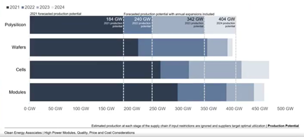
Perfect. Thank you so much, Michael. So, the first thing we really want to highlight in the move to larger wafers is where the current bottlenecks in the industry are in place. It should really be no surprise for anyone following into news. That polysilicon is continuing to be the hottest topic and the most limiting factor in the industry. Whereas much of the downstream sector would love to push out a large amount of large format products. There's just a limited amount of the raw material input that can really go in to producing a large number of modules for at least this year. so, what we have here on the chart is the expected production capacity, which is available at each stage of the manufacturing segment. This is ignoring any sort of material constraints. So obviously polysilicon there with the lowest amount of product output at around 184 gigawatts of solar conversion is a limiting factor for the rest of the industry.
Leading Manufacturers Across the Supply Chain are Moving to Embrace Large Wafers Causing Supplies to be Above Demand

What we're actually seeing as well as that polysilicon expansions, while underway are really not expected to come to fruition and reach full manufacturing capacity until about 2023. While the rest of the industry is really looking to continue expanding this year, next year, and even into 2023 and beyond in order to have a very large amount of production available for the solar industry. Switching to looking at just the top players, which are really pushing the change to the large format size conventions. We see that a lot of the changes actually is pushed by the wafer producers. So here at each stage of production, going from wafer, cell, and module, we have just the expected production capacities or expected nameplate capacities of the top five producers in the solar ecosystem. And so really if we focus on just the wafers in that left-hand chart for a moment, there's a tremendous amount of wafer concentration among a couple of wafer producers, which prefer either the 182-millimeter wafer format or the 210-millimeter wafer format.
Polysilicon’s Contribution to a Module’s Cost Remains Relatively Consistent no Matter the Module Layout

And the preferences of these wafer providers are really dictating the rest of the downstream industry from cell to module in adopting and switching to these larger wafer products. And what we'll get into is just a minute is what is actually the cost advantages for changing at each level of the supply chain. But really a lot of these players are also quite vertically integrated, especially your players like LONGi and JINKO here, which have not only the wafer processing, but a sizable amount of cell and module processing as well. So, they can have a complete ecosystem and really plan for the use of their preferred wafer format.
And so, jumping to a cost to price buildup of the different wafer formats, at least out the polysilicon level. There's almost an equivalent amount of savings gains from switching from a smaller format ingot to a larger format ingot. So, your smaller format ingots are slightly more efficient. There's lower kerf loss when you're forming the ingot for your 166, and 182 products, an ingot, and the 182 products actually has the lowest kerf loss because these different ingots and wafers will have a rounded corner. So, when you're slicing the different blocks, you'll actually have less product wasted. While the 210 is a square ingot, square format product. You might have some additional cutting loss because when you're cutting these ingots, you won't have that nice round shape when you're trying to get the square ingot block. But the larger cut pieces will allow for greater recycling rates for anything that has shaved off of the ingot block. So, you're really going to get about an equivalent cost per Watts, going from either a 166 millimeter and ingot wafer all the way up to a 210-millimeter ingot and wafer. Where the real differences start to emerge is in moving up to the wafer processing component. And this is why we've really seen the switched to large format, product being dictated and pushed by those big, very concentrated wafer producers. And so, while going to a larger wafer does require more energy and has a slightly higher cost during processing. You're getting a higher power product with the same throughput and basically the same efficiency in your manufacturing process. And so, the additional input or the additional output with a relatively low-cost base will give a lot of room for additional cost savings, which these wafer producers almost immediately eat up and some very high profit taking. This is of course, a little bit tempered by the current state of the polysilicon price ecosystem, but in the long-term, this will allow a lot of wafer producers, a much better profits ecosystem and a much better long-term profit outlook when they push either a 182 or a 210-millimeter wafer format.
Large Wafers are Preferred by Wafer Suppliers as they have more Room for Margin as Larger Wafers Enable BOS Savings

And when you go up to the cell level, you're also going to get some additional costs as your larger cells will require some additional materials, but just like you have with the wafers, there's a little bit less profit taking going on. And the higher throughput efficiency you get by having the same amount of cells produce but now, you have a higher power cell product, it will allow you some additional cost savings.
Cell Processing Becomes more Cost Efficient with Larger Sizes as Power-Per-Throughout Outweighs Additional Material Inputs

So that actually the cost per what goes down when you are using a 210- or 182-millimeter cell in relation to a 166 or even lower format cell. But to kind of round out the cost basis, when you actually get to the module material side, at least in the current ecosystem on the current state of material prices, you're really getting back to an equivalent cost per watt throughout the entire value chain.
Larger Modules may need Higher Quality Inputs, but also Provide Area Related Cost Savings which Produce Balanced Material Costs

As you go from polysilicon to cost, your larger format, modules will likely need some additional higher quality equipment, higher quality inputs to deal with the additional formats, you know, format difficulties such as some higher currents or some other parameters that need to be adjusted as you go to a larger format, but there are also your area related savings in going to a larger format product. And at least from the module perspective, some of the balance of system savings that are expected with a larger format product aren't necessarily revealed through the module manufacturing process. So many of the additional benefits of switching to a large format product that George highlighted earlier in this presentation are captured kind of outside the module manufacturing state.
Long Term Price Projections Forecast 182 mm Modules and 210 mm Modules will Converge at Approximately the Same Price Point

And what this might mean then for the consumer is that over the long term, it's expected that whether you have a 182-millimeter product or a 210-millimeter product, you're going to get about the same price per watt in the marketplace. This has been exasperated by the current state of having a ton of additional wafer selling module production and a very price sensitive demand base, which is looking at pushing out some products or pushing out some projects due to the rising cost of modules and forcing a lot of your producers to really compete on price in order to either promote their own format factor in the marketplace or continue to sustain sales. So, we're seeing any sort of price delta between your 182 and 210 products really start to evaporate, especially as we move into the end of this year, when we're likely to get a tremendous amount of new manufacturing capacity on the market, but not necessarily the amount of demand to support that additional manufacturing capacity. And I think we have just a couple minutes left. Michael, if you have any other questions or prepared closing statements.
Michael Schmela:
Yeah, let's take the time for questions. So, what about, so what do you see actually now, how that turns out in the market, the further development, so if we look at, for example, ITR PV, there are international technology roadmap for a PV. They lean more towards 182 for the next two years. While if you look at the roadmap profitable tech industry association, actually they lean more towards 210 where they think even capacities this year, next year are mostly 210 already the majority. So, with you being in the markets, seeing all these factories, checking actually what's coming out there, what are you seeing actually in terms of development?
Joseph Johnson:
From a manufacturing capacity perspective, at least you're going to have about an equivalent amount of your 210 wafer cells and module products, and the same as your 182-millimeter wafer selling module products. So, you really have Zhonghuan promoting the 210 and a lot of emerging players. So, you have Xuan Leon with a sizable amount of 210 capacity, wafer capacity coming online. Gouging solar, another new player in the wafer production space. And these new players all tend to prefer the 210-millimeter format, but they do have some ramp up that they need to, that needs to go on. So, these additional 210 wafer capacities aren't likely to materialize until 2022, whereas JINKO and Longi the main proponents of the 182 formats have a lot more wafer for production online now. So, we're likely to see a boost in 182-millimeter product available immediately this year, but into 2022, the balance between those two different formats in those camps from a capacity perspective should be about equivalent.
Michael Schmela:
Okay. And if we look at the demand side, actually, what do clients want? Because of course, you look at rooftop who wants all these big modules actually. And if you even look at a big power plants, so depending on how automated your installation teams are, it's also somewhat of an effort to have these big modules. So, what are you seeing there because you work usually for, developers, EPBCS help them sourcing their product? So, what's their preferences?
George Touloupas:
I'll take this one, sorry, because it really depends on the project. So, in some projects, one format might work better than the other. And so, there's no straight answer. There's no clear winner and also, its availability, right? So, it's not, there is no clear straight answer. And by the way, the residential product using G12 wafers, you just have to make them the right size. So, the wafer size can also make a big way for making small products.
Michael Schmela:
Okay. Maybe a final question. I think so market-based, so at snack we heard, for example, on the one hand we see increasing inventory and warehouses in China, on the other hand, it's hard for companies to get modules or they are pretty much high priced. So, can you maybe shine a little bit light on that from, from your experience? So, joseph has also shown actually that the silicon shortage will prevail for quite some time actually. But we have now also this Xin Juan issue and the new ban and the US so if we look at all these boundary conditions, what can we expect in terms of for projects in the west. So, it doesn't matter if it's an India in Europe or in the U S, what can we expect in terms of availability and pricing from modules of, let's say, over the next six months?
Joseph Johnson:
Next six months, we're starting to see pricing stabilize. So at least for the last two weeks polysilicon prices haven't increased, and we've seen a small decrease for the first time in months. So, it looks like for the rest of the year, barring some additional incidents in your polysilicon and production base, prices should be stable. So at least suppliers will have clarity to pass along to buyers about what the price will be. That doesn't mean prices will decline. As you mentioned, there is a significant amount of product in inventory, and that is true. And a lot of this product has been produced during the ecosystem or during the fear period where wafers and polysilicon were continuing to appreciate in price week on week, and many producers went ahead and bought your modules or produced cells, produced modules with the fear that the input costs would continue rising.
So, there's a lot of this very high priced, high costs inventory that is produced and sitting there waiting for a buyer. And because suppliers want to offload this high-cost inventory, they're really not willing to drop prices, even as some other cost basis components might start to fall, and this will hold true for the rest of the year. And then in addition, there's always the Q4 demand rush that we saw in 2020 and the domestic market is really counting on again in 2021 to offload a lot of that inventory, too. So, they are comfortable with having an above average amount of inventory on hand with the hope and the expectation that this will continue to get built out by the end of the year, as your large Chinese centric, government affiliated developers in the domestic Chinese market will pursue a project even at a higher cost if it gets down to it by the end of the year.
Michael Schmela:
Okay. Maybe final question. So, if you look at this environment, where do you think we will end up in terms of global shipments? Will it be the 160 gigawatt or so, I think IHS is still at 180 or where will we end up? What do you think? If we look at the current market environment.
Joseph Johnson:
Again, there's a lot of products that has already been made. And so, what we're looking at right now is a demand floor of about 150 gigawatts of installation. So, we should still get a boost over what was installed in 2020, but this ceiling could go all the way up to that polysilicon bottleneck of 180 gigawatts. There's a clear demand for product, but the price is just really pushing more and more projects into 2022. But a lot of projects have already been pushed into 2021. So, some developers are willing to bite the bullet and continue to go ahead with a project at a lower margin, even with a higher cost product. So just to reaffirm 150 to about 160, I think, is a realistic target, but this could always, of course have significant upside.
Michael Schmela:
Okay, cool. Any final statement from your side?
Joseph Johnson:
I think that is all for me, unless George wants to add anything.
George Touloupas:
I would like to say that these are exciting times. There's a lot of risks. There's a lot of fever, so we need to have very good intelligence and very good on the pricing and market and also on the technology side to make the right decisions. So, this is becoming more and more critical as opposed in the old times where modules were all the same, everything was stable. So, it was very easy to choose and take procurement decisions. This is not the case now.
Michael Schmela:
Thanks to everyone joining us. So maybe final words from me. So, if you're interested and not yet a member of Solar Power Europe, please join us. Clean Energy Associates is also very active. We have working streams on operations, maintenance on transparency, sustainability. So, all these topics that are hot these days we would be happy if you would work with us or with Clean Energy Associates. Thanks for joining and have a nice day. Thank you for having us.


